
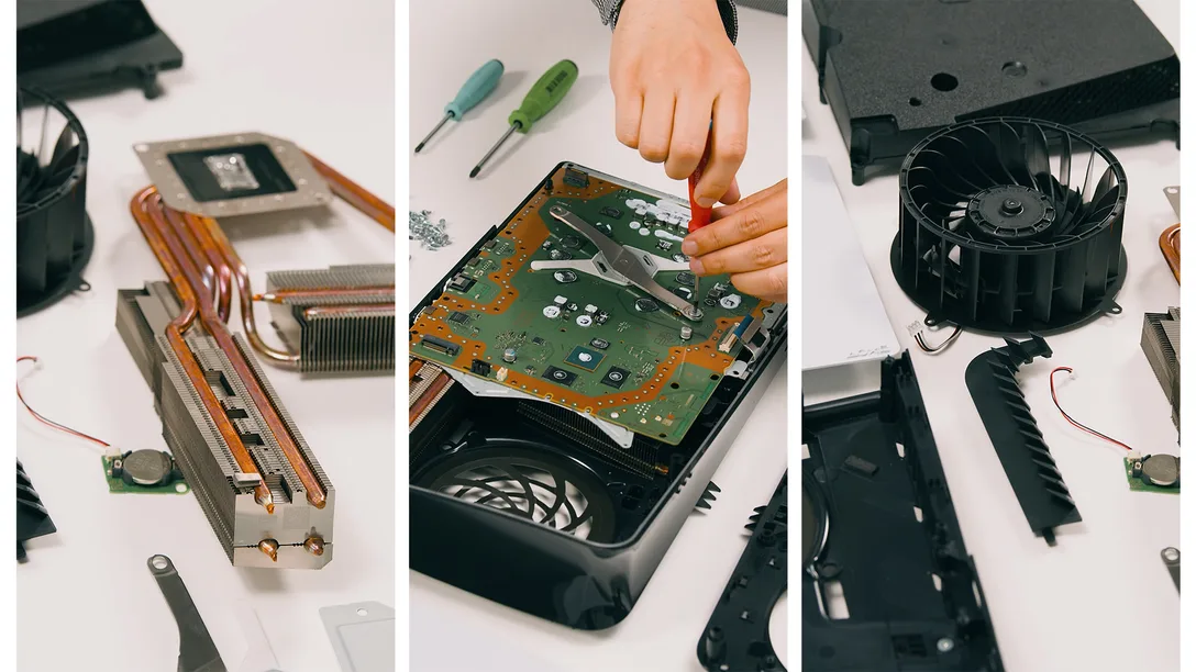
PlayStation recently revealed in a new official blog post a complete PS5 Pro teardown that offers a great look at the device internal hardware, and what innovation and tech Sony invested in to create its latest and most likely the last PlayStation 5 upgrade.
The PlayStation 5 Pro is Sony’s most advanced console to date, featuring substantial upgrades in cooling, performance, and internal design. The teardown, led by Sony engineers Shinya Tsuchida and Shinya Hiromitsu, offers a detailed look into the Pro’s engineering.
PS5 Pro Teardown highlights
Here is a complete rundown of all the important information from the blue team’s post:
-
New “blades” (three horizontal airflow slits) improve ventilation and are a visual hallmark.
-
Louver structures reduce fan noise, particularly in the direction players face.
-
A larger fan with redesigned blades moves more air while staying quiet.
-
The heatsink has more heat pipes and a carefully optimized layout for efficient thermal dissipation.
-
Motherboard is larger and includes more circuits to support enhanced specs.
-
PS5 Pro adds a 9th RAM chip (DDR5) for background processes, freeing the faster 8x GDDR6 for gaming performance.
-
The System-on-a-Chip (SoC) enables high-res, high-frame-rate gameplay using AI-powered PlayStation Spectral Super Resolution (PSSR).
-
PS5 Pro continues to use liquid metal TIM for the main processor, with added grooves for better stability.
-
This decision stems from anticipating the future of high-density semiconductors.
-
A larger PSU (power supply unit) provides ~48W more output.
-
Integrated support for Wi-Fi 7, making PS5 Pro one of the first consoles to adopt this fast standard.
PS5 Pro Teardown Photos


As many of you already know, the PS5 Pro is Sony’s most advanced hardware to date, so it’s no surprise to see this much innovation packed into the device. But if you’re looking for a more detailed look at its capabilities, performance, and price value, we recommend checking out our complete PS5 Pro review.